In today’s era of rapidly evolving network communication, equipment such as 5G base stations, data centers, and communication modules are facing unprecedented demands in terms of system stability, signal integrity, and thermal performance. Effectively resolving both thermal and electromagnetic interference (EMI) challenges has become a top priority for electronic system designers. Leveraging its deep expertise in thermal and EMI materials, NFION has introduced an innovative Thermal Absorbing Pad, integrating dual functions of heat conduction and electromagnetic wave absorption. This disruptive solution offers comprehensive protection for high-speed communication systems.
1. Dual-Function Design: One Pad Solves Two Problems
Conventional designs often address thermal management and EMI shielding separately—thermal pads or gels for heat, and absorbers or shielding structures for EMI. However, this segmented approach not only complicates assembly but also increases the risk of EMI leakage due to material stacking.
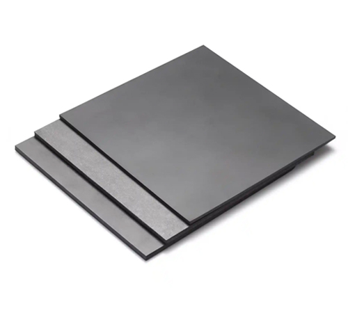
NFION’s thermal absorbing pad redefines this approach. With a precise formula combining thermally conductive elastomers and high-loss magnetic particles, it delivers synergistic heat dissipation and EMI absorption. The pad can be directly applied to heat-generating and EMI-prone components—such as SerDes chips, switch ICs, optical modules, and RF front ends—solving two challenges with one material.
2. Key Features: Setting a New Benchmark for High-Frequency Materials
Beyond integrating functions, NFION’s thermal absorbing pad delivers exceptional performance:
▪ Thermal conductivity: 2.0–5.0 W/m·K, suitable for medium-to-high power components;
▪ Wideband absorption from 1GHz to 40GHz, covering 5G, mmWave, Wi-Fi 6/7, and more;
▪ Soft and compressible, with low modulus to accommodate uneven surfaces and reduce mechanical stress;
▪ Available thickness: 0.5mm–5.0mm, suitable for varying structure designs;
▪ Customizable sizes, adhesive backing, and protective coatings for reliable integration.
Its outstanding thermal and EMI performance makes it a forward-looking solution for the miniaturization and high-frequency trend in communication devices.
3. Versatile Applications Across Communication Frontiers
NFION’s thermal absorbing pad has proven performance in a wide range of scenarios:
▪ 5G base station antenna units: absorb EMI resonance, ensuring signal stability;
▪ Data center switches: suppress EMI leakage from high-speed SerDes;
▪ Automotive modules (C-V2X, mmWave radar): withstand harsh environments while managing heat and EMI;
▪ Industrial and military radar systems: meet dual challenges of EMC and thermal reliability.
Validated by leading communication companies, this product demonstrates robust reliability in real-world deployment.
4. NFION’s Customization Capabilities: Built for Performance
With in-house formulation and vertically integrated production, NFION offers tailored thermal absorbing pad solutions based on customer-specific TDP, frequency, assembly gap, and mechanical requirements. Customization options include formula adjustment, shape/thickness, adhesive lamination, and environmental sealing.
NFION also provides full technical support—thermal and EMI simulation, system-level validation, and reliability testing—ensuring faster design-in and enhanced product stability.
5. Conclusion: Materials Driving the Future of Connectivity
As communication technologies evolve toward higher speeds, greater integration, and smarter systems, materials are no longer just passive components—they’re enablers of next-generation performance.
NFION’s thermal absorbing pad breaks traditional boundaries with its all-in-one design, offering a more efficient, reliable, and simplified path for EMI and thermal control in communication devices.
NFION will continue to lead innovation in thermal and EMI material convergence, partnering with global clients to power safer, more stable, and cooler digital connections.
 CN >
CN >